Analog PLLs & DLLs

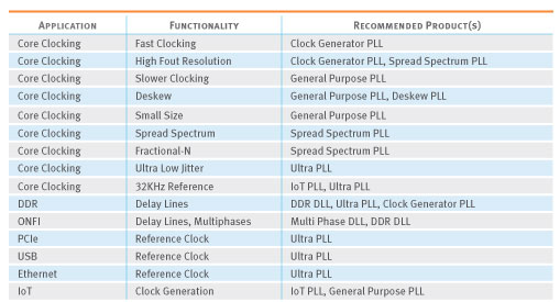
True Circuits offers six general categories of low-jitter PLL hard macros: Ultra PLLs, IoT PLLs, General Purpose PLLs, Clock Generator PLLs, Spread Spectrum PLLs, and Deskew PLLs. We also offer low-jitter Multi-slave DDR DLL and Multi-phase DLL hard macros. These hard macros have excellent jitter performance while operating in the hostile mixed-signal noise environment present in today's ICs. They span nearly all performance points and features typically requested by ASIC, FPGA and SoC designers. Our PLLs support wide frequency and multiplication factor ranges, ultra low jitter and are fully pin programmable. Our DLLs have excellent linearity, very high resolution and are ideal for high-speed DDR and other interface applications. These PLL and DLL hard macros are available in TSMC, GLOBALFOUNDRIES and UMC logic processes from 180nm to 4nm.

True Circuits now offers a PLL specifically tailored to the stringent power requirements and wide frequency operation range of the rapidly-growing IoT market. Sipping only 45uW at 30MHz and running from core power, the IoT PLL is designed for very low power. With multiplication factors up to 8192, the PLL is able to run off of a small and inexpensive 32KHz crystal and still clock a 32-bit CPU at up to 250MHz. The IoT PLL is ideal for applications like wearables and senor devices, where the power-performance profile must be managed tightly, and possibly over a very wide frequency range.

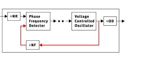
True Circuits offers a state-of-the-art PLL that uses high-speed digital and analog circuits to achieve exceptional performance, with many useful features. The Ultra PLL is highly programmable so one PLL can be used for all applications on a SoC. It has ultra-low jitter performance (<500fs) and ultra wide multiplication range (1-250,000). It offers precise frequency control with a least 26 fractional bits (at least 10 precise) for extremely high fractional-N resolution. The PLL can also generate precise and adjustable frequency spreading with programmable rate and depth to meet tight FCC requirements.

Digital PLLs & DLLs

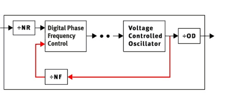
True Circuits has introduced new synthesizable PLLs and DLLs that will continue to raise the bar for timing IP features, performance and flexibility for a wide range of customer applications. Since 1998, TCI has led the industry with the regular introduction of new timing architectures and IP design types that have defined the timing IP category, and offered chip designers a wide variety of solutions to their timing needs. TCI is proud to offer our latest timing IP, the synthesizable Precision PLL, micro PLL and micro DLL. Each is available in the latest process nodes and back to 28nm.

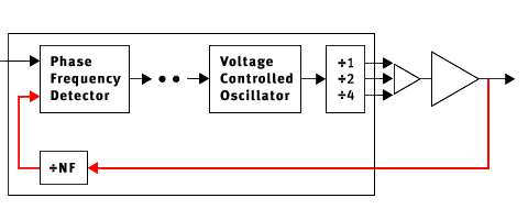
The synthesizable Precision PLL generates multiple precision clocks supporting any modulation scheme from almost DC to 10GHz. The outputs can be independently dynamically programmed cycle-by-cycle to any clock period and the clock frequency can be a precise ratio of floating point numbers times the reference frequency. The integrated phase noise is better than 500ps RMS. It is ideal for SerDes, processor and DVFS applications.

The synthesizable micro PLL is a small synthesizable general-purpose PLL that multiplies the reference clock by any integer or fractional-N value from 1 to 500K. It supports reference clock frequencies as low as 32KHz and output frequencies as high as 3GHz. It can stay locked to the reference clock while it changes over a 10:1 frequency range. Because it is synthesizable, it can support spreading as well as other modulation profiles. It is relatively low power, very fast locking and can quickly restart from a sleep mode.

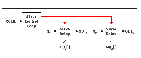
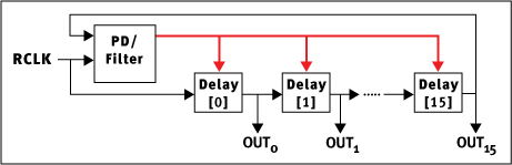
The synthesizable micro DLL is a small synthesizable DLL with a master and multiple slaves topology. It can support reference frequencies typically in the range of 500MHz to 3GHz and track reference changes over an 8:1 frequency range while providing 9-bit accuracy in slave delay programming. Slave delays can be changed glitch free and the DLL can quickly restart from a sleep mode. It has a very small zero code offset that can be precisely cancelled.

True Circuits' continuous product improvements and product additions are driven by lab experience, customer requirements and our unique understanding of real world timing applications.


To assist you in selecting the right PLL or DLL for your chip application, the following table offers a product selection guide. For a downloadable version, see the TCI Product Summary.


The Ultra PLL is designed with a state-of-the-art architecture using high-speed digital and analog circuits that offers exceptional performance, features and ease of use. It is highly programmable so one PLL can be used for all applications on a SoC. It has ultra-low jitter performance (<500fs) for the most demanding SerDes and ADC reference clocks. It has ultra wide frequency range with multiplication factors over 250,000 to support reference clocks from 32KHz to 1GHz. It has precise frequency control with a least 26 fractional bits (at least 10 precise) for extremely high fractional-N resolution. It can generate precise and adjustable frequency spreading with programmable rate and depth to meet tight FCC requirements. It draws low power in a compact size.


The IoT PLL is designed for very low power, sipping only about 45uW at 30MHz and running from core power. It has a wide frequency range with multiplication factors up to 8192, allowing the PLL to run off of a small and inexpensive 32KHz crystal and still clock a 32-bit CPU at up to around 250MHz. It is ideal for IoT applications like wearables and senor devices, where the power-performance profile must be managed tightly, and possibly over a very wide frequency range.


The General Purpose PLL is a wide range clock multiplier with deskew capability. It contains a 1-16 divider at the reference clock input, a 1-64 divider in the internal feedback path, and a 1-16 divider at the output. The outputs are 50% duty cycle for all output divider values. It delivers optimal jitter performance over all multiplication settings and is suitable for system clock, DDR and general purpose applications where small size, low power and low cost are important.


The Clock Generator PLL is designed to multiply an input clock by an integer between 1 and 4096. It does not provide any deskew functionality. It contains a 1-64 divider at the reference clock input, a 1-4096 divider in the internal feedback path, and a 1-8 divider at the output. It supports fractional-N multiplication with additional external low speed logic. The outputs are 50% duty cycle for all output divider values.


The Spread Spectrum PLL is designed to multiply an input clock by a fixed-point number between 92 and 184 with frequency spreading capability suitable for PC and consumer electronics applications that require low EMI. It does not provide any deskew functionality. It contains a 1-64 divider at the reference clock input, a 1-256 or larger integer divider and a 1-256 or larger fractional divider in the internal feedback path, with as many as 4 bits of precise fractional-N control, and a 1-8 divider at the output. It can generate precise and adjustable frequency spreading depths (1.5% typical and up to around 10%) and rates (30KHz typical). The outputs are 50% duty cycle for all output divider values.


The Deskew PLL is designed to eliminate the skew between the output of a clock distribution tree and a clock reference. The PLL can also multiply the clock reference by an integer between 1 and 4. It provides three 50% duty cycle skew aligned outputs that are divided down from the internal VCO frequency by 1, 2, and 4.


The DDR DLL uses a reference clock to establish a time base in order to delay arbitrary (nonperiodic) strobe signals by precise fractions of the clock cycle. It uses a phase-locked analog delay line which rejects temperature and supply voltage variations, and has high supply noise rejection for very low jitter operation. TCI can configure this block to have almost any number of slaves (which delay the arbitrary signals) with a single master section (which establishes the time base) to minimize area and power. The slave delays can be independently set to precise values or dynamically adjusted after determining the boundaries of a data eye. The DDR DLL has excellent linearity and very high resolution. TCI can also configure this block to output multi-phase clocks directly from the reference clock.

The analog delay-line architecture used in our DLL design sharply contrasts with those used in digital DLL approaches. The analog control loop allows our DLL to continuously and smoothly compensate its delays to changing voltage and temperature conditions, without any quantization jitter or output glitches. However, digital delay-line control loops, which typically multiplex between inverter outputs along a string of inverters, must select between quantized delay values. Such approaches can lead to imprecise delays and either output glitches from updates or timing drifts from voltage and temperature variations in the absence of updates. The analog delay line used in our DLL design is internally isolated from supply noise for very low output jitter, while digital delay lines tend to be very supply noise sensitive as they convert it percent-for-percent into output jitter. Our analog delay line also provides pulse width compensation to minimize pulse width distortion, unlike digital delay lines. Finally, our DLL design provides very high digital adjustment resolution (typically 7 bits), where the steps are precise fractions of the clock period, unlike digital DLL designs where the adjustment steps are very large and not well calibrated.


The Multi Phase DLL is designed for high-speed interface applications. The DLL generates precise multi-phase clocks directly from the reference clock. It delivers optimal jitter performance over a wide frequency range. The analog delay-line architecture used in our DLL design is internally isolated from supply noise for very low output jitter. The analog delay line also provides duty cyle correction.


Copyright © 2002-2023 True Circuits, Inc. All Rights Reserved